The Challenge
Increased demand for large scale displays and smaller screens for mobile devices, is driving the development of new ways to produce high resolution display structures. The challenge for Hi-Accµracy is to develop cost effective display structures adaptable to a wide range of applications.
Hi-Accµracy's Solution
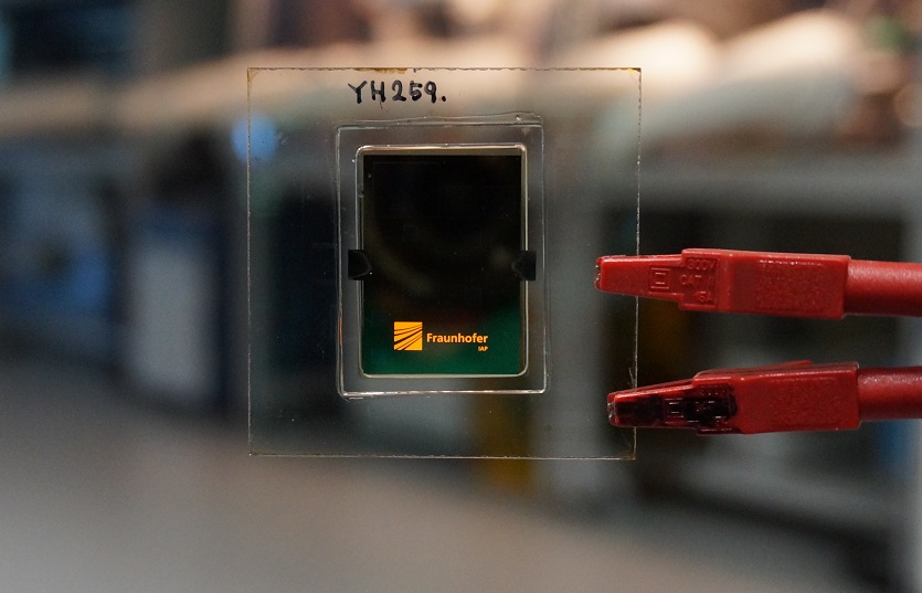
Hi-Accµracy will develop flexible, high resolution display structures, that can be produced at low cost with minimal environmental impact. The project aims to utilize a range of low-temperature curable nano-Ag and nano-Au conductors and p-type organic semiconductors. It will also develop InP, ZnSe and ZnS Quantum Dot materials and electroluminescent EL-QD-LED material stacks and barrier layers that can achieve required WVTR and oxygen transmission rates.


Impacts
The Hi-Accµracy team will review state of the art designs, components and production methods. Based on emerging requirements the partners will produce turn-key materials required for the manufacture of the OTFT structures so that each of the Hi-Accµracy’s layers and interlayer interactions optimise OTFT performance. This will set new standards for display quality and open up new applications for flexible, high resolution screens across multiple sectors. Specific attention will be paid to reducing the environmental impact of the technology, for example, by minimising the use of solvents.
Methodology
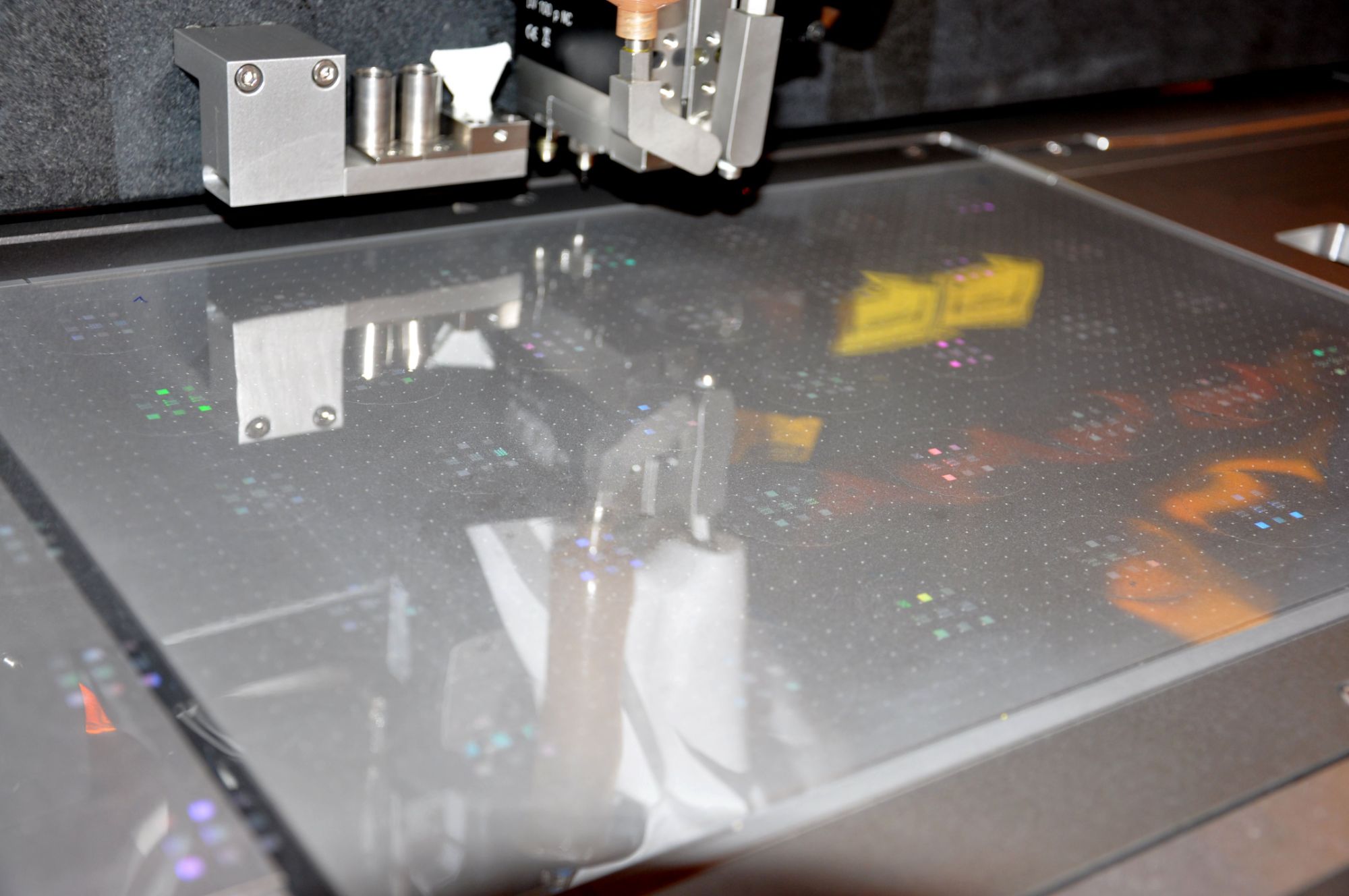
Hi-Accµracy aims to fundamentally address the development of cutting-edge non-vacuum processing technologies to create structures with very high resolution, down to the μm-scale. These key central processing technologies are scalable, cost-effective and will ultimately enable large-area manufacture of flexible OLAE (Organic & Large Area Electronic) structures.
- Electrostatic Jet Printing (ESJET)
- Nano-Imprint Lithography (NIL)
- Reverse-offset printing (ROP)
- Electrostatic Spray Assisted Vapour Deposition (ESAVD)
- Assisted Ion Deposition (AAID)
- High Resolution Stencil and Screen Mesh (HRSSM)