Consortium

Hi- Accµracy is an ambitious, 3.5 year, project comprising a pan-European EU consortium of 11 world leading research centres and cutting-edge SMEs that will develop and commercialise these technologies. SONY, Huawei and Polar, three major global electronics companies have endorsed the project and will act as the project’s External Expert Advisory Board.

The 11 members of the consortium are:


https://www.joanneum.at/ 

JOANNEUM RESEARCH (JOR) (Forschungsgesellschaft mbH) is a leading Austrian innovation- / technology-provider with approx. 450 employees and has been practicing research on an international level for over thirty years. Joanneum will be responsible for project coordination and technical management and will also lead the integrative work packages for specification (WP1) and demonstrators (WP7).  JOR will employ NIL to aid ESJET in reaching unprecedented levels of resolution and precision in the µm and sub-µm scale.


https://pvi.co.uk/index.php/research-development/

PVI has a strong background in the development and manufacturing of innovative sensor systems, primarily for the automobile industry.  PVI R&D is a leader in high precision printing and will focus primarily on ESJET printing and material characterization. PVI have manufacturing facilities to produce the integrated printing system based on the ESJET.  PVI will also work closely with other partners to lead the dissemination and market development activities for the project.


https://www.vttresearch.com/en

VTT is a national technological research centre in Finland with a wide spectrum of activities. In particular, VTT focuses on microelectronics, sensors and integrated systems. Particularly relevant for this proposal is the fact that VTT specializes in developing manufacturing processes and technologies for flexible, light, large area, high volume electronic devices and systems.

VTT will be involved in; the development of the high-resolution printing technique reverse offset (ROP) for deposition and patterning of interconnects and electrodes for oTFT devices in particular; the development of the technique for deposition of organic materials developed in the consortium; the development of high-resolution oTFTs and backplanes for the demonstrators developed in the project. In addition, a key task for VTT will be to facilitate the development of shared specifications for the different manufacturing technologies developed, to ensure the practical realization of demonstrators as well as a viable industrial process for future full-scale deployment.

www.smartkem.com

SmartKem is seeking to reshape the world of electronics with a revolutionary semiconductor platform that enables a new generation of displays, sensors and logic. SmartKem's patented TRUFLEX® inks are solution deposited at a low temperature, on low-cost substrates to make organic thin-film transistor (OTFT) circuits. The company's semiconductor platform can be used in a number of applications including miniLED displays, AMOLED displays, fingerprint sensors and integrated logic circuits. SmartKem develops its materials at its research and development facility in Manchester, UK, and its semiconductor manufacturing process at the Centre for Process Innovation (CPI) at Sedgefield, UK. The company has an extensive IP portfolio including over 175 patents across 17 patent families. For more information, visit: www.smartkem.com and follow us on LinkedIn SmartKem, Inc. | LinkedIn  and Twitter @SmartKemTRUFLEX


https://www.iap.fraunhofer.de/en/fraunhofer-iap.html


The Fraunhofer IAP specializes in researching and developing polymer applications. It supports companies and partners in the customized development and optimization of innovative and sustainable materials, processing aids and processes. In addition to characterizing polymers, the institute also produces and processes polymers in an environmental-friendly and cost effective way on a laboratory and pilot plant scale.
Within Hi-Accµracy, Fraunhofer IAP will lead the development of quantum dot based inks for the processing of electroluminescent QD devices. This includes material development towards highly efficient materials for the three colours red, green and blue based on non toxic QDs, as well as QD-LED stack optimization with appropriate hole injection/transport and electron injection/transport materials. In cooperation with IMEC/Holst RGB AM-QD-, LEDs will be fabricated directly on the active matrix backplane.


https://www.dycotecmaterials.com/

Dycotec Materials Ltd (DML) develops and manufactures advanced electrically and thermally conductive, dielectric and overcoat materials for a wide range of applications including sensors, photovoltaic, semiconductor, automotive and display. We provide over 50 different types of materials globally from small to large volume. DML will utilise its expertise in advanced materials ink formulation to develop the material sets needed for the different layers of the backplane for both the ESJET and Reverse off set (ROP) printing processes required within Hi-Accuracy.


https://www.hu-berlin.de/en

Humboldt-Universität zu Berlin was founded in 1810. Since 2012 it has been one of 11 universities of excellence in Germany. The Hybrid Devices Group has been affiliated with the Departments of Physics and Chemistry as well as IRIS Adlershof since its inception in 2015.

HU Berlin will focus on the electrical characterization of materials and device interfaces: work function, valence band, XPS, conductivity, (FET mobility) and the characterization of lab-based devices and TCEs, process control and development.


https://www.ucl.ac.uk/

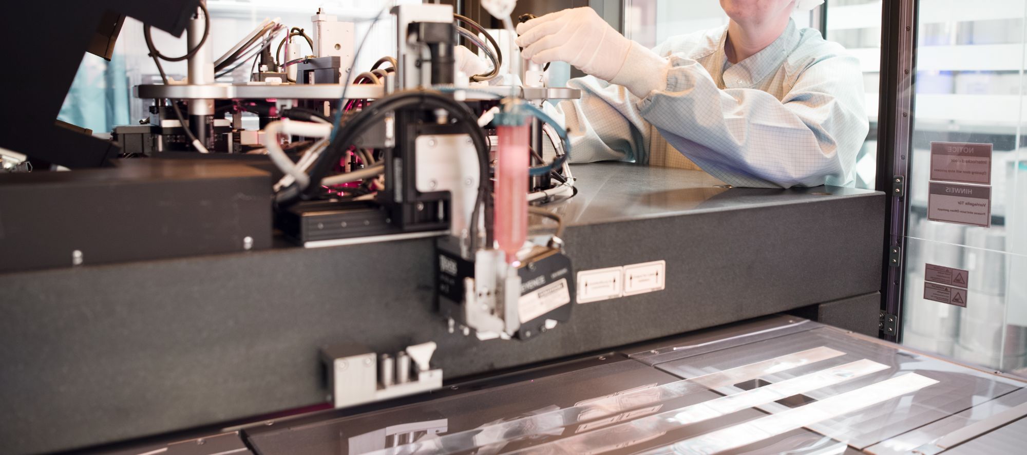
University College London (UCL) has a global reputation for excellence in research and is committed to delivering impact and innovations that enhance the lives of people worldwide.  The role of UCL in Hi-Accuracy includes the contribution to multilayer barrier, p-type OSC, TFT structures, conducting electrodes as well as dissemination.  UCL’s tasks include project planning and technical coordination involving the following and lead the workpackage /tasks on:
(i)  The development of efficient methods for the manufacturing of multilayer barrier, p-type OSC, OTFT based structures, interlayer and conducting electrodes;

(ii)  Fabricating the test structures;

(iii) Materials characterisation and validation;

(iv) Develop and manufacture non-vacuum prototype coatings & solutions, including their integration into novel printed electronic systems, in collaboration with industrial partners using novel, cost-effective methods, integrating with ESJET and solutions that have been developed in the above.

(v) Market and technology take-up planning with project partners and Future Research Road Mapping, which targets the full exploitation of Hi-Accµracy results.


https://www.imec-int.com/en/home

IMEC is one of the largest independent R&D institutes world-wide, with an international staff of over 2000 people of 70 different nationalities.  IMEC is contributing to the consortium as the display technology architect. IMEC will work with the consortium to define the final display specification layer by layer to demonstrate the desired performance of each printing technology developed in Hi-Accµracy.

The main tasks of IMEC are to design the peripheral electronic system to drive the display demonstrator and to contribute to the design and verification of AMQD-LED /AMOLED display realized with a-IGZO TFT backplanes.


https://www.crf.it/EN

With a full-time workforce of more than 850 highly trained professionals, Centro Ricerche FIAT (CRF) is an industrial organization having the mission to promote, develop and transfer innovation for providing competitiveness to FIAT Chrysler Automobiles (FCA). 

CRF will be involved in:

·       Definition of the specifications of automotive market and demonstrators for flexible formable display for ALFA ROMEO and high premium brand MASERATI project.

·       Testing of materials in terms of structural robustness, chemical resistance surface and interface analysis.

·       Validation and Final assessment of the vehicle component following FCA standard.

·       Evaluation of manufacturing process for the automotive sectors.

·       Exploitation within the automotive market and transfer to Tier1, Tier2 and SI.

HI-ACCURACY perfectly matches CRF’s expertise and targets because surface technology and integration of electronics is a key technology for automotive sector. Within GML division, the technical unit “opto-electronics” allows the validation and assessment of the materials and vehicle components in such direction. Within the involved laboratories, the validation of demonstrators between suitable materials, the manufacturing phases, the curing as well as the final assessment of demonstrators will be carried out.


https://www.bnn.at/

BioNanoNet Forschungsgesellschaft mbH (BNN) is a non-profit scientific network that specializes in the Key Enabling Technologies nanotechnology and biotechnology, with emphasis on (nanotoxicology,  sensortechnology, as well as health, (nano-)safety and (nano-) medicine.

BNN will develop an integrated (nano-)safety strategy to reduce the potential risk upon worker’s exposure to manufactured nanomaterials (MNM) during the project.  Their activities include nanosafety assessment, Safe-by-Design implementation, interaction in the nanosafety-community on international level (e.g., EU NanoSafety Cluster), as well as dissemination and outreach activities.